
Overview
Organizations
- HOME
- >
- Recent events
010
Yoshida Laboratory in Department of Electrical Engineering understands and controls process of high-performance superconducting films by analyzing the process information.
High-performance superconducting films are required for fusion and electric aircraft applications. To fabricate km-long superconducting tapes with maintaining high properties, the film fabrication process should be controlled. Pulsed laser deposition is one of the industrially used fabrication methods for the superconducting tape. We observe, analyze, and predict the plume image in pulsed laser deposition to understand and control the process of the superconducting film.
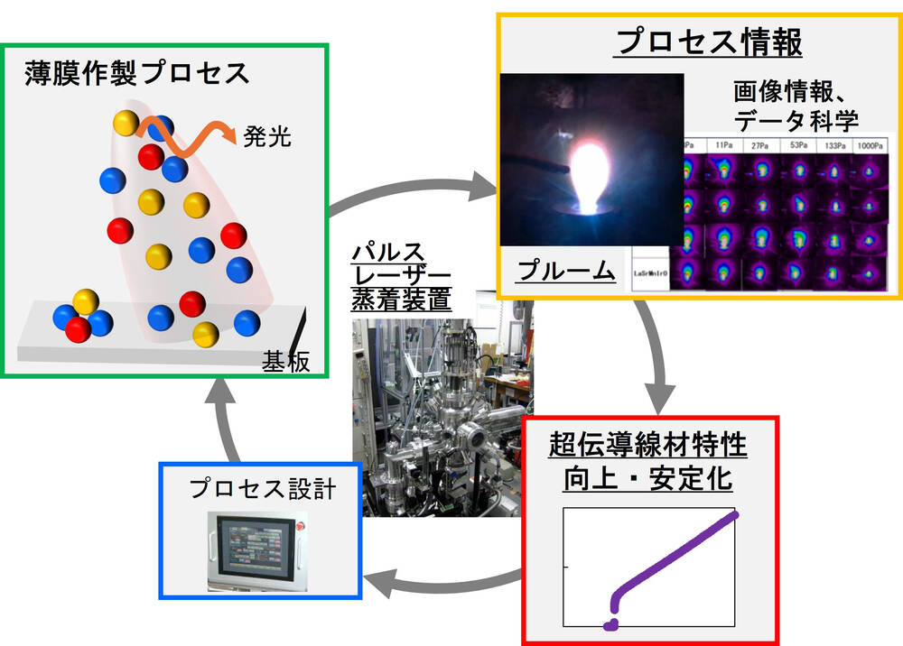
- Schematic of process information based design for superconducting film process
009
Sato & Ogawa Lab. in the Department of Information and Communication Engineering studies on a novel operation interface for a teleoperated social robot
In existing operation interfaces for teleoperated social robots, operators often face the problem of high workloads and boredom caused by monotonous operations. We have therefore developed a new interface that allows the operator to actively operate the robot while having fun by applying the concept of gamification. We implemented an interface with functions such as buttons making a robot speak and a point-earning feature, and demonstrated that operators actually enjoy operating robots through field experiments at a shopping mall.
Details are here
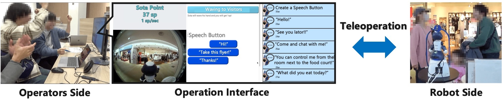
- Overview of robot operation interface applying gamification
008
Nishizawa Laboratory in Department of Electronics is working on the development of freely-controllable optical frequency comb and its application to innovative environmental spectroscopy measurement technology.
In Nishizawa Laboratory, we are developing new highly functional, freely controllable optical frequency comb light sources with the aim of realizing innovative environmental spectroscopy measurement technology. Recently, we have developed a new ultrashort pulse fiber laser that places a molecular gas cell or a liquid crystal spatial light modulator inside the oscillator, and have succeeded in generating a high level of spectral peaks within the oscillator, and have clarified the physical mechanism behind this.
[1] N. Nishizawa, S. Kitajima, and Y. Sakakibara, "Spectral peaking in an ultrashort-pulse fiber laser oscillator with a molecular gas cell," Optics Letters, vol.47, no.10, pp.2422-2425 (2022).
[2] S. Kitajima, S. Kobata, and N. Nishizawa, “Programmable spectral peak generation by a mode-locked Er-fiber laser with an intracavity LCOS-SLM filter,” Optics Letters, vol.49, no.22, pp.6529-6532 (2024).
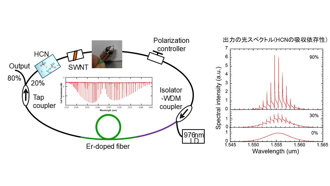
- The configuration of an ultrashort pulse fiber laser containing a molecular gas cell and a carbon nanotube, and the spectrum of its output beam. We have succeeded in generating highly narrow linewidth spectra that match the absorption wavelengths of the molecule. By using a spatial light modulator, a spectral peak can be generated at any wavelength.
007
The Ohno Laboratory, Department of Electrical Engineering, has developed a new tomography method based on simple measurements.
As part of our research on fusion power generation, which is expected to be a future energy source, we have developed a new measurement and analysis method combining tomography and statistical methods, and clarified the 4-dimensional spatiotemporal behavior of plasma transport phenomenon that is enhanced when the heat load on the device wall is reduced.
Details are here
Details are here
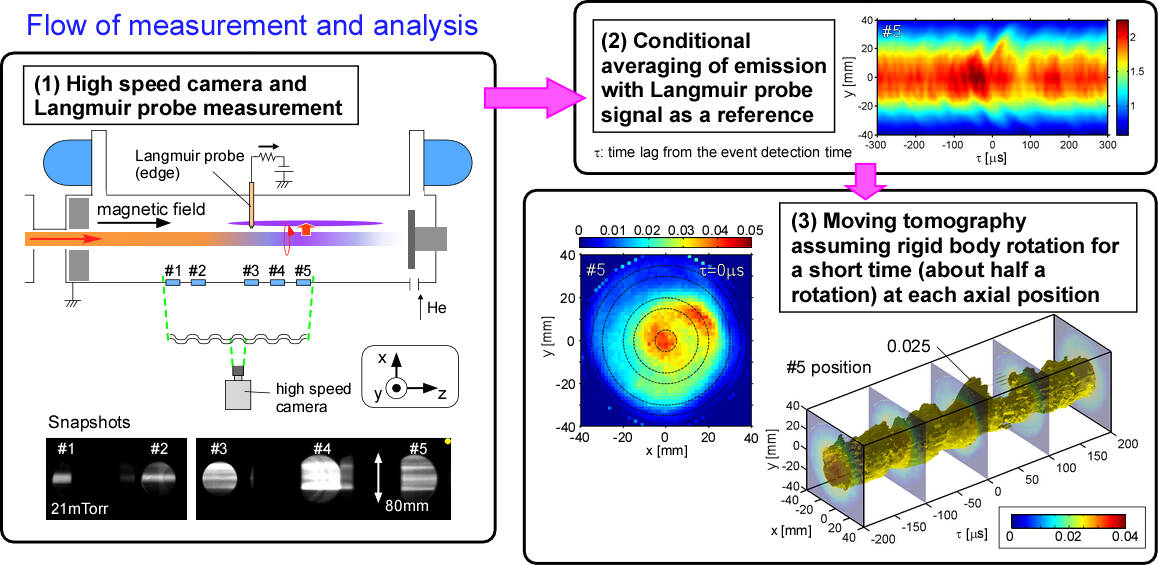
- Fig. Flow of measurement and analysis and the spatiotemporal transport structure of plasma revealed in the linear plasma device NAGDIS-II.
006
Makihara Laboratory is working on Si-based semiconductor quantum dots, and their process technologies to develop novel functional Si-based devices operating with a few electrons or photons over room temperature
To contribute enhancement of functionality of silicon nanotechnology, we are studying cross-disciplinary research in the rang from materials science to process integration and device technology. In particular, we are developing technologies to control the size and density of Si quantum dots in the self-assembled formation of SiH4 and GeH4 gases by LPCVD, as well as developing new functional devices.
Details are here
Details are here
Details are here
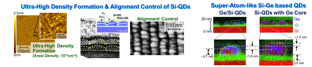
- Formation & Characterization of Si-based QDs
005
Takeyoshi Kato Laboratory of the Department of Electrical Engineering has been developing a model to promote charging electric vehicles using surplus electricity from renewable energy sources.
Electric vehicles (EVs) can run without CO2 emission if EVs are charged with surplus power from renewable energy sources. To investigate a required scheme for EVs to contribute a carbon neutrality, we have developed a model for calculating EV charging demand depending on various future scenarios(1). The developed data is utilized for analysis of future supply and demand in various distribution networks(2).
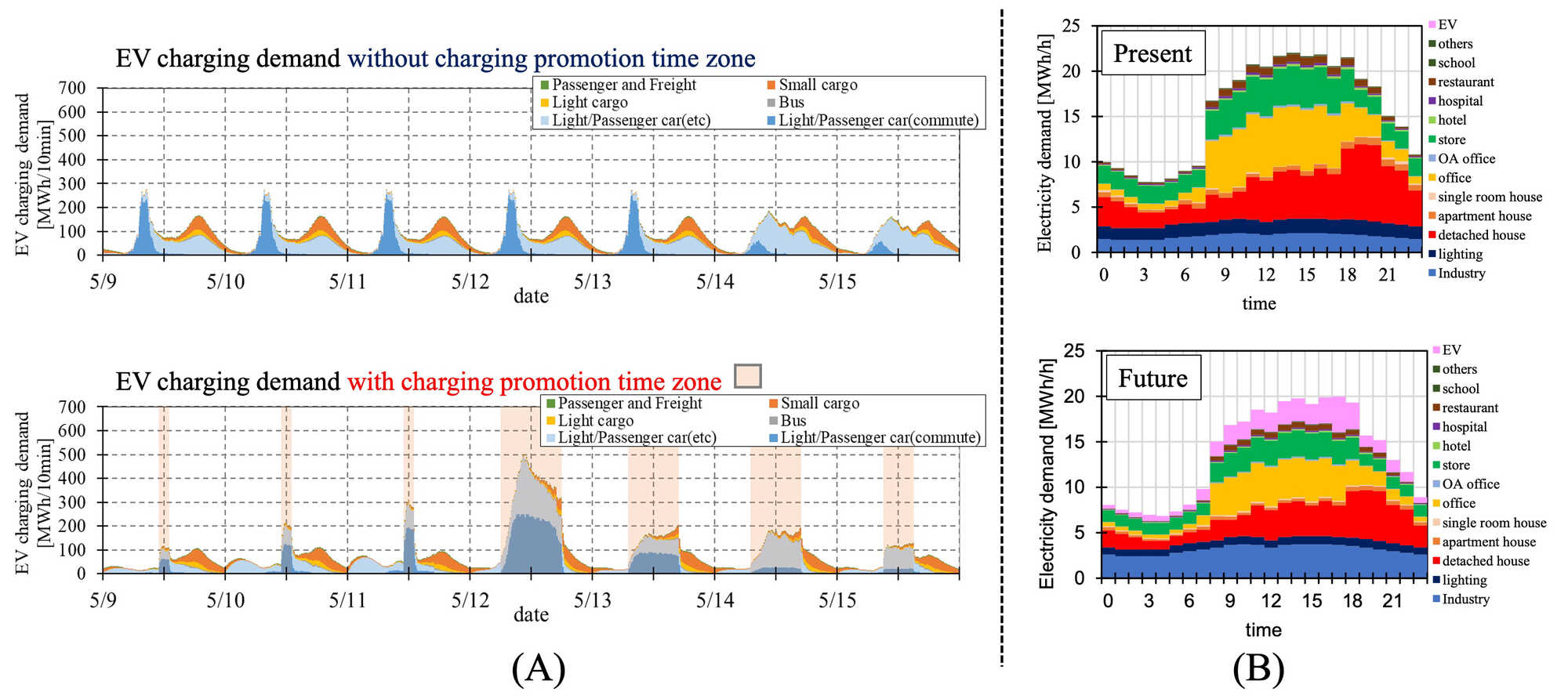
- (A) Introduction of charging promotion time zone to promote charging with renewable energy sources
- (B) An estimation of electricity demand (August) within the distribution system in City N, Gifu
004
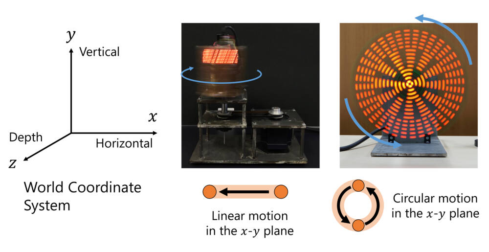
The World's first and only: Utilizing light trails, we achieved spatially high-capacity, high-degree-of-freedom parallel transmission in image sensor communication with a few light sources.
An image sensor is a camera's photosensitive device that detects different light sources individually and outputs them as an image. While it can receive many optical signals simultaneously, the transmitter requires many light sources or a large installation area. Controlling numerous light sources with high speed and precision increases design complexity and manufacturing costs. Additionally, fixed light sources limit the density and direction of signal transmission. We proposed the world's first and only parallel transmission method using light trails of moving light sources. This method achieves high-capacity, high-degree-of-freedom parallel transmission with few light sources and a small installation area, enabling multi-directional information transmission. This work has been published in IEEE Photonics Journal and Optics Communications [1][2].
[1] Z. Tang, J. Zheng, T. Yamazato and S. Arai, "Image Sensor Communication via Light Trail Using Propeller LED Transmitter," in IEEE Photonics Journal, vol. 15, no. 5, pp. 1-12, Oct. 2023, Art no. 7304412, doi: 10.1109/JPHOT.2023.3317082.
[2] Z. Tang, T. Yamazato, "Image sensor communication and its transmitting devices," in Optics Communications, vol. 541, 2023, 129545, ISSN 0030-4018, doi: 10.1016/j.optcom.2023.129545.
003
Uchiyama Research Group in the Department of Electronic Engineering is conducting research on the application of magnetic sensors to medical diagnosis and autonomous driving systems by developing ultra-sensitive, compact magnetic sensors.
We are developing ultra-sensitive compact magnetic sensors using amorphous magnetic wires to measure biomagnetic field associated with electrical activity in the heart and brain in aim of an applications to medical diagnosis. We are also developing a vehicle traffic measurement system for application to autonomous driving.
Details are here
Details are here
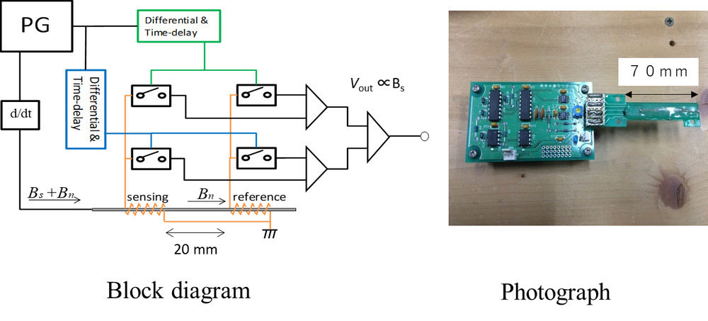
- Figure: Magnetic sensor system for biomagnetic measurement (Magnetoimpedance type gradiometer)
002
Okada research group has been developping wireless communication systems using drones in mountainous areas.
Okada Research Group investigated the feasibility of a self-managed wireless communication system using drones in mountainous areas. In order to provide stable communications between a base station and drones, the location method of wireless relay stations was proposed that takes into account the topography of mountainous areas, and the characteristics of radio propagation in mountainous areas are clarified through experimental measurements.
Details are here
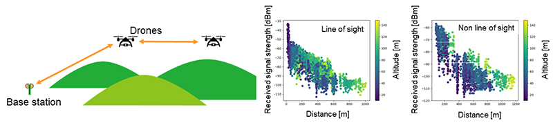
- Wireless communication systems using drones. Left: System model. Right: Wireless propagation characteristics.
001
Takahashi research group in electrical engineering has been developing new microscopy technology to reveal the functions of cells and materials at nanoscale resolution.
The Takahashi laboratory has been developing scanning probe microscopes based on nanoscale-sharpened glass pipettes to observe the nanoscale structure and function in biological samples and functional materials. In these cell biological applications, dynamically changing such as reagent uptake process can be observed at super resolution. In these material applications, nanoscale geometrical structures and electrochemical information can be visualized, which is useful for the development of highly functional materials.
Details are here
Details are here
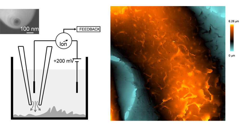
- Figure 1. Measurement principle of Scanning Ion Conductance Microscopy (left) and high-resolution imaging of cancer cell surface (right). Reprinted with permission from Y. Takahashi, et al., Anal. Chem. 2023, 95, 34, 12664–12672. Copyright 2023 American Chemical Society.
