
Overview
Organizations
- HOME
- >
- Electronics
Research Groups
Staff
Research field
Future Electronics Creation
Professor Giichiro UCHIDA
Associate Professor
Haruka SUZUKI
Our laboratory advances the development of novel plasma systems and translates them into real-world applications.
Industrial plasma applications/Plasma source development/Materials synthesis and processing/Plasma-based environmental technologies
 Novel-concept sputtering systems
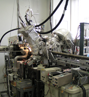
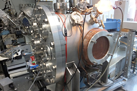
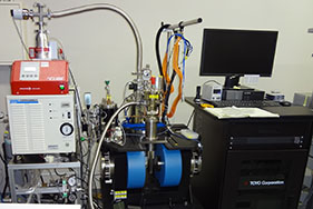
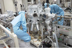
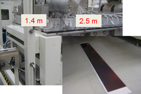 Meter-scale plasma generation systems
Professor
Kenji ISHIKAWA
Professor
Ngo Van Nong
Designated Professor
Makoto SEKINE
Associate Professor
Takayoshi TSUTSUMI
Assistant Professor
Kenichi INOUE
最先端プラズマナノ科学技術で拓く、環境・医療イノベーション
薄膜シリコン太陽電池 / カーボン太陽電池 / GaNパワーデバイス / 3色発光LED / プラズマ医療科学 / プラズマ滅菌・殺菌 / 農業・環境応用(小型成分分析装置) / プラズマ気相診断 / 新規プラズマ源開発
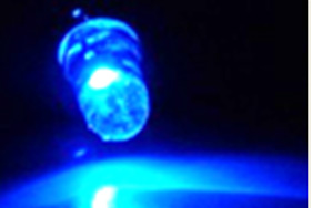
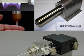 超高密度プラズマ源(上三図)
小型ラジカルモニタ(下図)
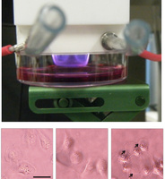
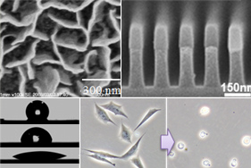 プラズマプロセスによるカーボンナノ材料の合成(上左図)・ナノメータ加工(上右図)・プラズマ処理によるカーボンナノウオール表面の超親水性?超撥水性制御(下左図)・プラズマ照射による卵巣癌細胞のアポトーシス誘起(下右図)
Professor
Hiromasa TANAKA

Associate Professor
Kae NAKAMURA
Creation of Life Electronics Contributing to Medicine, Agriculture, and the Life Sciences
Plasma Medicine / Plasma Agriculture / Plasma Molecular Biology / Plasma Chemistry / Life Electronics
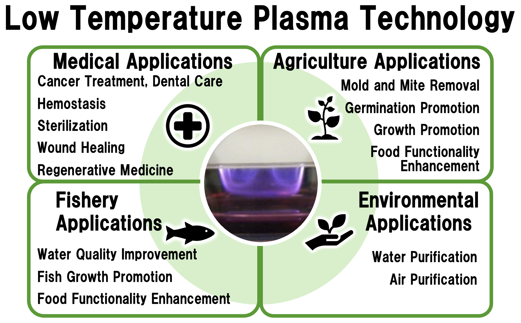 Low-temperature plasma technology is expected to be applied in various bio-related fields such as medicine, agriculture, and fisheries.
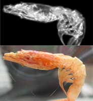
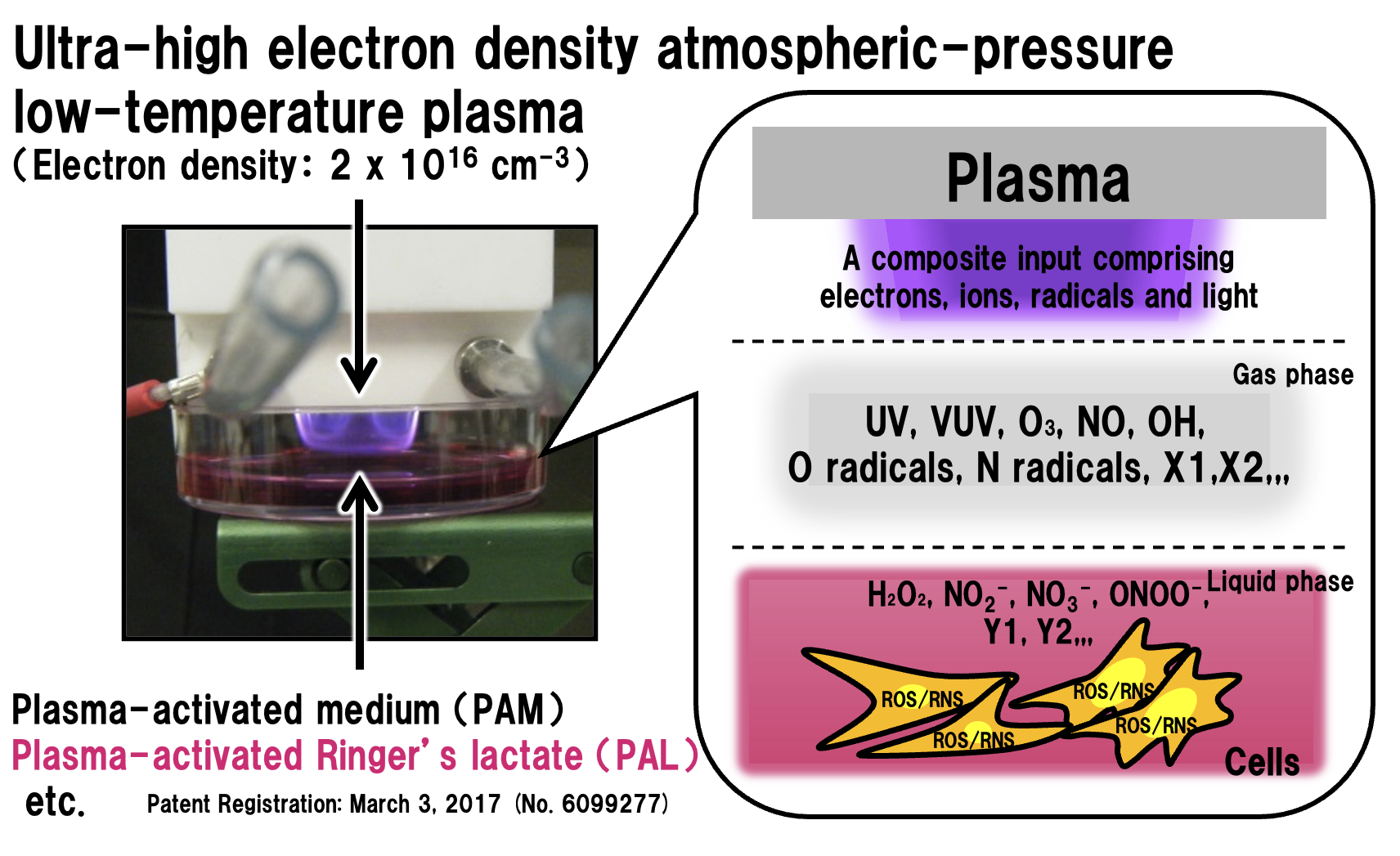 Solutions irradiated with plasma, which we have termed "plasma-activated solutions," have been found to exert various effects on cells, tissues, and organisms;
however, many of their underlying molecular mechanisms remain largely unknown.
Solutions irradiated with plasma, which we have termed "plasma-activated solutions," have been found to exert various effects on cells, tissues, and organisms;
however, many of their underlying molecular mechanisms remain largely unknown.
Information Device Engineering
Professor
Yasufumi TAKAHASHI
Lecturer
Hiroki IDA
Seeing the Invisible!
Next-Generation Microscopy Technology Pioneering Nano-Biosensing
Biosensors / Scanning Probe Microscopy / Super-Resolution Microscopy / Live Cell Imaging / Energy Storage Materials / Catalytic Materials
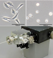
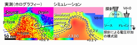
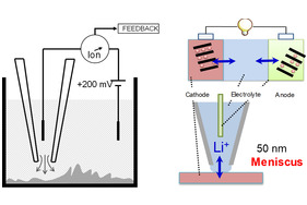 Overview of Scanning Probe Microscopy Using Nanoscale Glass Pipettes
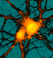
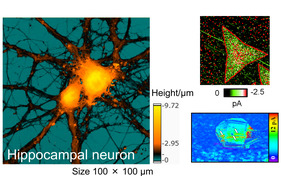 Using our self-developed microscopes, we are working to visualize the structure and function of nerve cells,
catalytic materials and rechargeable batteries at the micro- and nanoscale resolution.
Using our self-developed microscopes, we are working to visualize the structure and function of nerve cells,
catalytic materials and rechargeable batteries at the micro- and nanoscale resolution.
Professor
Katsunori MAKIHARA
Assistant Professor
Yuki IMAI
Through cutting-edge Si-based semiconductor research, you will tackle real-world challenges and issues while acquiring practical fundamental knowledge. In addition to collaborative research with international institutions and presenting your results at conferences, these experiences will help you develop the essential abilities required of independent engineers and researchers.
Si/Ge QDs / Super-Atom-like QDs / Alloy-NDs / GaN / Silicide / Control of the Crystalline Phase / Selective-Etching / High-Sensitive Defect Measurements / GAA / LEDs / FG-Memories / Sensing Devices
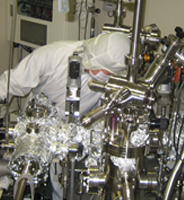
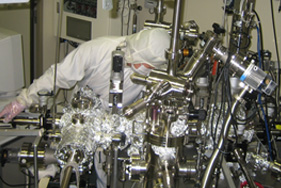 Quantum Dot Formation System
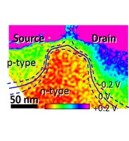
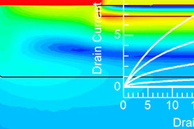
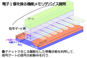 Schematic Illustration of a Multi-Bit Comparator Based on Si Quantum-Dot Floating-Gate MOSFETs
Professor
Jun SUDA
Designated Professor
Yuji ANDO
Associate Professor
Masahiro HORITA
Assistant Professor
Tomoya WATANABE
We are conducting research on next-generation power devices using novel semiconductor materials that will contribute to the realization of energy-saving electric and electronic equipment. Our research activities range from basic research on materials science and solid-state physics to applied research on device design and performance evaluation.
Wide-gap semiconductors / Power devices / Electronic devices / Semiconductor defect physics and defect control / Device fabrication processes / Device simulation / Severe environment devices
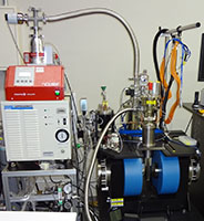
 Magnetic field modulated Hall effect measurement system with temperature control
 Design of high-performance power devices by device simulation
Quantum System Engineering
Professor
Norihiko NISHIZAWA
Lecturer
Shotaro KITAJIMA
Lasers, a cutting-edge technology in quantum optoelectronics, are used in a wide range of fields, from basic research to industry and medicine, and are expected to lead to the development of even more novel applied technologies. In this laboratory, we develop cutting-edge laser light sources and manipulate ultrashort pulsed light with extremely narrow durations to create even more novel technologies.
Laser / Optical fiber / Ultrashort pulse / Ultra-broadband light source / 3D optical tomography / Fiber laser / Medical optics and optical measurement / Optoelectronics
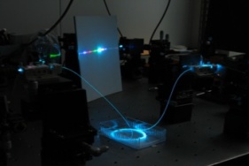 Generation of ultra-broadband light using optical fibers.
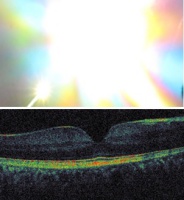
 Ultra-high resolution 3D tomographic images of porcine tracheal tissue observed using ultra-broadband light
Professor
Masamitsu TANAKA
Assistant Professor
Feng LI
We aim to create ultra-high-speed, low-power electronics by utilizing superconductors and realizing cutting-edge information processing circuits that operate near the physical limits.
Josephson devices / single flux quantum circuits / superconducting spin-electronic devices / next-generation computing / quantum information processing and computer systems
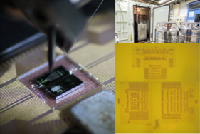 World’s largest-class superconductor integrated circuits toward next-generation supercomputers. We cooled down the chips in liquid helium and successfully obtained operation above 50 GHz.
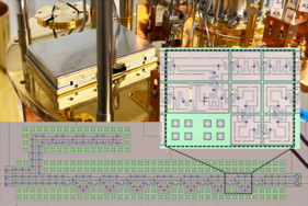 Single-flux-quantum circuits developed for controlling superconductor quantum bits. We employ extremely low-power design techniques to achieve 20-mK operation in a dilution refrigerator.
Professor
Kodo KAWASE
Associate Professor
Kosuke MURATE
Light for the future: Cutting-edge terahertz wave research
Terahertz wave sources / Terahertz imaging / Terahertz and bio / Terahertz sensing / Terahertz spectroscopy
 An injection-seeded terahertz parametric generator : Achieves world's highest brightness of 100 kW, surpassing free electron lasers,
in a tabletop size. Also achieves a high dynamic range of 10 orders as a terahertz spectrometer.
An injection-seeded terahertz parametric generator : Achieves world's highest brightness of 100 kW, surpassing free electron lasers,
in a tabletop size. Also achieves a high dynamic range of 10 orders as a terahertz spectrometer.
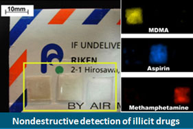 Non-destructive inspection of illicit drugs in mail using terahertz waves: Our terahertz spectroscopic imaging technology can detect drugs hidden
in envelopes and other packaging items. This new technology is expected to be used by customs and postal offices.
Non-destructive inspection of illicit drugs in mail using terahertz waves: Our terahertz spectroscopic imaging technology can detect drugs hidden
in envelopes and other packaging items. This new technology is expected to be used by customs and postal offices.
Nanoelectronics(Institute of Materials and Systems for Sustainability)
Professor
Yoshio HONDA
Associate Professor
Maki KUSHIMOTO
Designated Professor
Markus PRISTOVSEK
Innovating Materials and Devices with Nitride Semiconductors
We aim to develop a wide range of impactful applications,
including high-efficiency power devices for energy saving, high-frequency devices for the upcoming 6G era, and novel ultraviolet laser sources for medical, pharmaceutical, and sterilization uses.
Energy saving & generation / Quantum effects & novel functionalities / Nitride semiconductors / Compound semiconductors / Crystal growth / Optoelectronic devices / μ-LED / Laser diodes / Power devices / High-frequency devices
 packaged blue LED
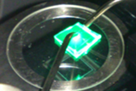 fabricated green LED chip
Professor
Takeshi KATO
Associate Professor
Daiki OSHIMA
Development and application of nanomagnetic materials, and research on advanced nanodevices that utilize electron spin as an information carrier
Nanomagnetics / Information Storage / Spintronics / Solid-State Magnetic Memory / Micro Magnetic Sensors / Energy Devices Utilizing Magnetic Materials
 [8 Sources Magnetron Sputtering]
Magnetic thin films with nanometer-scale thickness are fabricated using a sputtering system. The chamber equipped with eight material sources, enabling the deposition of multilayer structures for functional spin devices.
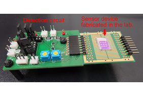 [GMR Magnetic Field Sensor]
Highly sensitive magnetic field sensor based on giant magneto-resistance (GMR) effect. The sensor device was microfabricated to control the domain wall motion in the free layer of the GMR film, and was incorporated into a detection circuit to realize high sensitivity.
Our laboratory is dedicated to exploring novel devices based on fundamental studies of physical properties. We employ advanced transmission electron microscopy techniques, which enable the direct visualization of electromagnetic fields with atomic- and nanoscale resolution.
Nano-scale electromagnetic field analysis/Structural analysis/Interface properties/Research and development of novel functional devices and materials
We are developing novel nano-electron devices based on low-dimensional materials such as carbon nanotubes and two-dimensional materials towards next generation semiconductor electronics. Flexible biomedical devices are also the target of our research.
Nanomaterials / Carbon Nanotubes / Atomic Layer Materials / Nanodevices / Semiconductor devices / Flexible Devices / Biosensors
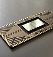
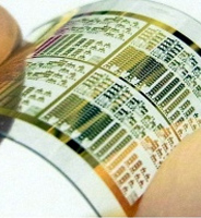
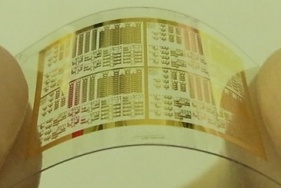 The world's first carbon nanotube integrated circuit fabricated on transparent plastic. Unlike conventional
silicon-based semiconductors, the CNT flexible IC is lightweight and flexible.
The world's first carbon nanotube integrated circuit fabricated on transparent plastic. Unlike conventional
silicon-based semiconductors, the CNT flexible IC is lightweight and flexible.
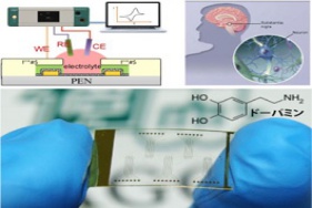 A biosensor fabricated with carbon nanotubes. It can detect neurotransmitters present in the central nervous system such as dopamine with high sensitivity.
