
Overview
Organizations
- HOME
- >
- Recent events
005
High-precision angular distribution measurement technique in semiconductor etching plasma is newly developed
As one of research topics, Toyoda Lab., Department of Electronics, is pursuing analysis of etching plasmas used for semiconductor fabrication processes. In Flash Memory fabrication, high-aspect-ratio (close to 100) hole etching is commonly used and ion directionality control to meet with such high-aspect-ratio etching is required. However, there have been no high-precision measurement technique to evaluate angular distribution of high energy ions impinging on the wafer surface. We have newly developed a unique measurement device to measure angular distribution of impinging ions with using a imaging technique, and have succeeded in measuring ion angular distribution within an error of 0.1 degree, and also succeeded in measuring angular distribution of high-energy neutral atoms. This result will provide vey important information on the guideline for the plasma control and contribute to the improvement of memory performance in the future.
Details are here
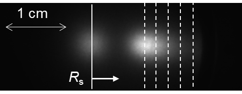
Typical image of ion and neutral beam measurement
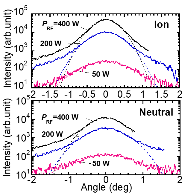
Angular distribution measurements of ion and neutral beams in etching plasma source.
004
Research on selective doping for p-type gallium nitride utilizing ion-implantation and ultra-high-pressure annealing
To realize the green society, Suda Laboratory has been developing power semiconductor devices, which used in power conversion systems. Gallium nitride (GaN), one of the widegap semiconductors, has attracted much attention as a next-generation semiconductor to reduce the energy loss in power conversion. Selective area doping using ion-implantation is one of the important techniques in the fabrication of power device structures. However, realization of p-type GaN by ion-implantation has been big challenge. We have developed ultra-high-pressure annealing (UHPA) technique, where the high-temperature annealing for implanted GaN is performed under ultra high pressure. Recently, we have revealed that p-type GaN can be formed under the UHPA conditions of 1300°C and 300 MPa, the pressure of which is as low as practical use. This work was presented in International Workshop on Nitride Semiconductors 2022 (IWN2022, Oct. 2022, Berlin, Germany).
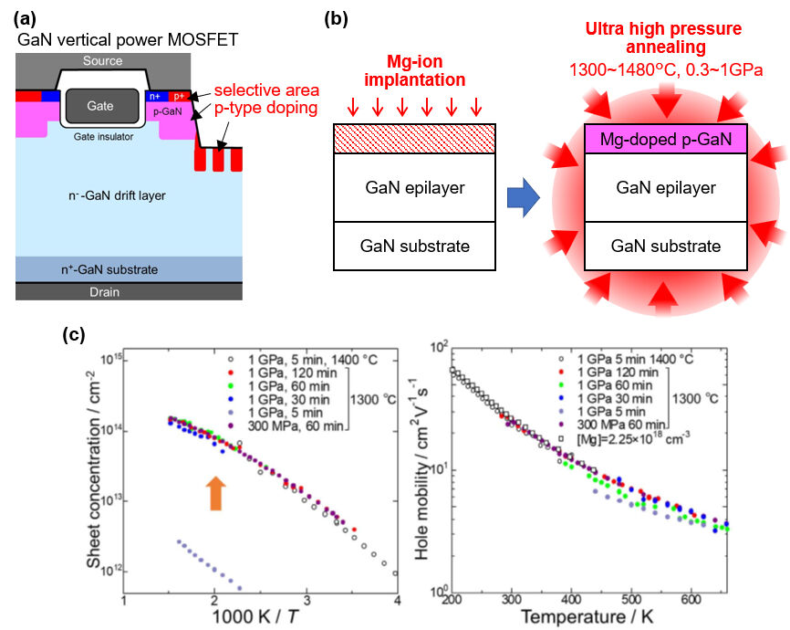
(a) Usage of p-type selective doping in vertical power devices. (b) Fabrication process of p-type GaN using ion-implantation and ultra-high-pressure anneal, (c) Temperature dependence of hole concentration and mobility for the GaN measured by Hall-effect measurement. Implanted GaN layers annealed at 1300°C and 300 MPa for 60 min showed p-type conductivity which was equivalent to epitaxially grown p-type GaN layers.
003
Research on triboelectric energy harvester as a power source for wearable electronics.
Ohno Laboratory is developing soft wearable devices that are in harmony with humans using carbon nanotubes, which have excellent mechanical properties and electrical conductivity. Such wearable devices are expected to be powered using energy harvesting technology, which generates electricity from small amounts of energy in the environment. We developed soft triboelectric nanogenerators that generate electricity from human motion.
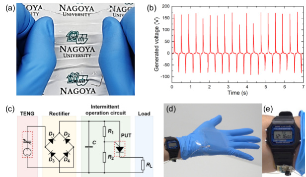
Fabricated triboelectric nanogenerator (a) and the generated voltage (b).
The photograph of driving a wristwatch by hand clapping (d,e) by using the intermittent operation circuit (c).
002
A new display robot for connecting physical space and virtual space was newly developed.
As virtual reality expands, new means of communication are required to connect and integrate physical and virtual spaces.
Kawaguchi Laboratory is developing a new mobile robot called MetaPo that combines a spherical display, a 360-degree camera, an AMR (Autonomous Mobile Robot), and IoT actuators, and is developing a method to connect arbitrary spaces with each other. The first result of this research was presented at the international conference ACM SIGGRAPH held in Vancouver in August.
Details are here
Details are here
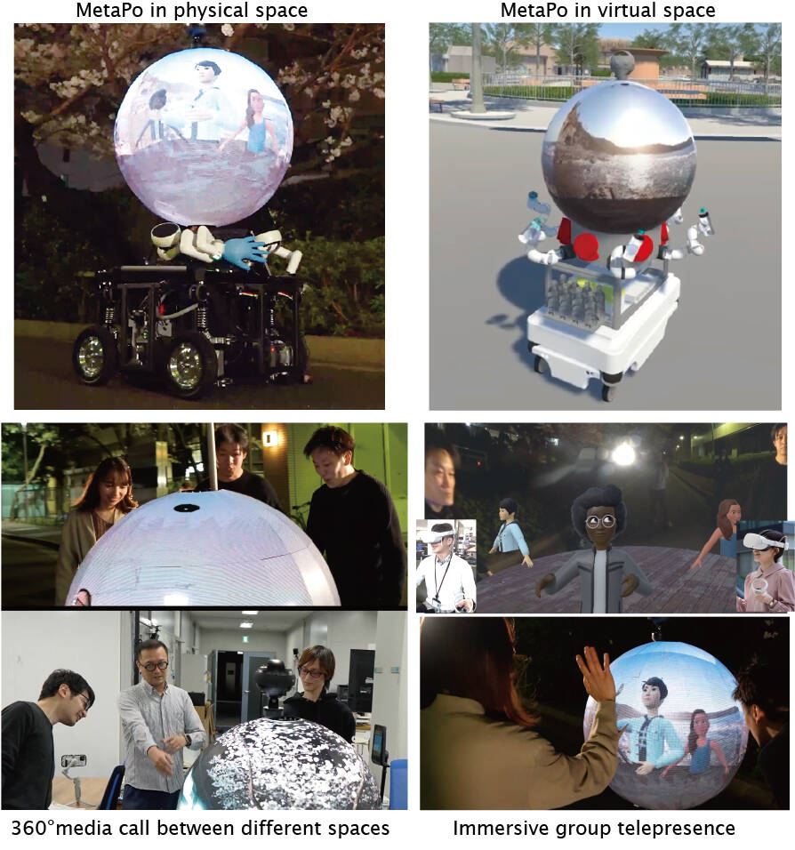
The developed mobile display robot called MetaPo and the communication using MetaPo.
001
Research on physical properties of semiconducting materials for realizing next-generation energy devices. (Ikarashi Lab. IMaSS)
Our research interest includes developing next-generation energy device materials for the realizing a sustainable society. For example, introducing impurity atoms into semiconductor crystals and controlling their distribution (doping) are key process for the fabrication of semiconductor devices. Using state-of-the-art analytical equipment at Nagoya University, we are developing technology to measure and control the distribution of impurity atoms and defects in the crystal with atomic resolution.
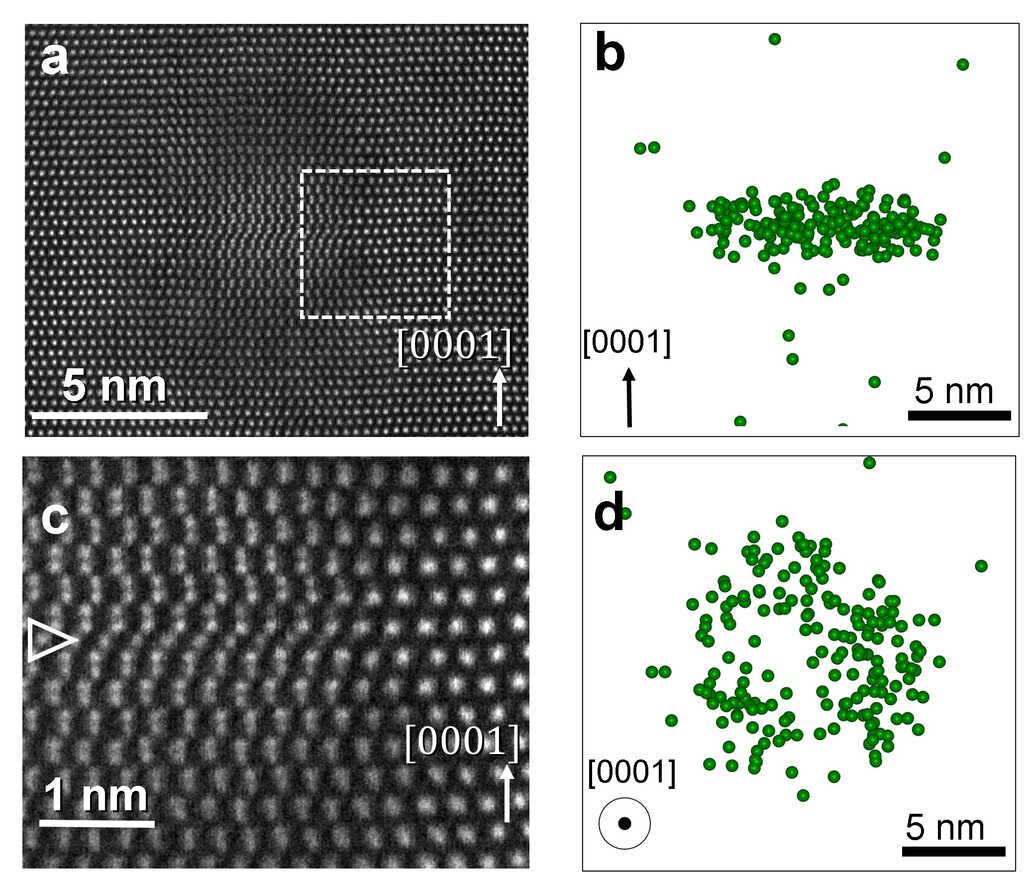
Observation of a GaN crystal defect and impurity atom (Mg) distribution.
- a Each bright spot shows a Ga atom. Atomic arrangement is disordered in the center of the figure. The arrow points to the GaN crystal surface.
- b Impurity atom (Mg) map around the defect. The green dots are Mg atoms.
- c Magnified image of the dotted area in Figure a. An excess Ga atomic plane is seen at the position marked with ▷ in the defect.
- d The Mg atom map seen from the crystal surface direction. Mg atoms are distributed in a donut shape around the defect.
